Research
Two-qubit cryo-CMOS control of a spin register in diamond
Overview Research area: Quantum computing hardware — specifically, cryogenic classical control electronics (cryo-CMOS) co-integrated with spin qubits in diamond. Technical level: Advanced. The paper a
- arXiv
- 2610.26413
- Published
- 2026-10-19
- Authors
- H. B. van Ommen, N. E. Fakkel, M. van Riggelen, J. Yun, L. A. Enthoven, M. A. B. ElBadry, F. Sebastiano, M. Babaie, T. H. Taminiau
AI summary
Overview
Research area: Quantum computing hardware — specifically, cryogenic classical control electronics (cryo-CMOS) co-integrated with spin qubits in diamond.
Technical level: Advanced. The paper assumes familiarity with spin qubits, hyperfine interactions, dynamical decoupling, gate set tomography, and RF/mixed-signal IC design.
Scope: The paper reports single- and two-qubit control of an electron spin and nearby carbon-13 nuclear spins in nitrogen-vacancy (NV) centres in diamond, driven entirely by a cryo-CMOS application-specific integrated circuit (ASIC) operating alongside the diamond chip at 6 K.
What This Paper Is About
Scaling quantum computers to the ~10^6 physical qubits cited for fault tolerance (or ~10^4 for some architectures) means the room-temperature rack of control electronics becomes a bottleneck: cabling, heat load, and sheer channel count. One proposed fix is to move the control electronics into the cryostat as custom silicon. This paper asks whether such a cryo-CMOS chip can do more than simple single-qubit experiments — specifically, whether it can execute the pulse sequences needed for a genuine two-qubit entangling gate between an electron spin and a nuclear spin in diamond.
Key Contributions
-
Two-qubit control from a cryo-CMOS chip. The authors integrate a cryo-CMOS qubit controller with a diamond NV device in a cryostat and use it to drive an electron–nuclear two-qubit gate, estimating an average gate fidelity of F_2q,avg = 95(2)% and a Bell-state fidelity of F_state = 88.6(8)%.
-
A dual-band, single-coil architecture. The chip contains a GHz signal generator for the electron spin and a MHz signal generator for up to 10 nuclear spins, sharing one drive coil patterned on the diamond device, with a switchable matching network that optimizes the impedance for either GHz or MHz driving.
-
Rigorous single-qubit benchmarking with Gate Set Tomography. GST is used to characterize the electron spin and two carbon-13 nuclear spins, and the fitted error generators are analyzed to identify which noise processes limit each gate.
-
A co-design analysis of electronics and physics requirements. The paper lays out the interplay between CMOS design choices and NV-centre control requirements, and identifies concrete priorities for future chip iterations (timing resolution, MHz-generator noise, heat dissipation).
Main Findings
-
Electron-spin drive strength: The Class-DE RFDAC reaches a peak current over 80 mA_p, producing an electron-spin Rabi frequency of 2.31(1) MHz. Nuclear-spin Rabi frequencies lie between 1 and 2 kHz.
-
Coherence under dynamical decoupling matches room-temperature equipment: Using XY8 sequences with up to N = 512 pulses, the electron-spin state is preserved up to 50 ms. A power-law fit T_2^e = T_0·N^η gives T_0 = 1.1(2) ms and η = 0.62(3). Measurements with the room-temperature system and the CMOS chip powered off show comparable performance, indicating the GHz generator does not degrade coherence.
-
Anomalous decoherence scaling at fixed pulse spacing: At fixed τ = 1.460 µs, the coherence decay fits e^{-(N/N_0)^2} with N_0 = 1.8(1)×10^3 better than the e^{-N/N_0} form expected from nuclear-spin bath noise, suggesting an additional noise source inside or outside the diamond.
-
Single-qubit fidelities: Electron-spin average gate fidelities exceed 99%, with the worst gate at 99.26(8)%. For the nuclear spins, average gate fidelities are above 99.4% for c_0 and 96% for c_1. GST data were considered up to germ length L = 16 (electron), L = 8 (c_0), and L = 2 (c_1).
-
Error generators point to different limits per qubit: For the electron identity gate (pure XY8 decoupling), stochastic z error dominates. For the electron π/2 gates, stochastic x and y errors dominate, possibly indicating amplitude fluctuations. For c_0, both gates show significant under-rotation (coherent x/y error), which the authors attribute to an amplitude drift or systematic calibration error.
-
Two-qubit gate calibration: DD spectroscopy with N = 44 pulses reveals a resonance with a linewidth of ~4 ns at τ_e = 1.3507 µs, from which A_∥ = 31 kHz and A_⟂ = 130 kHz are extracted. The fully entangling point occurs at N = 28 pulses, implemented as 3 XY8 sequences and 1 XY4 sequence.
-
Timing resolution is a limiting practical factor: The sequencer clock was raised fourfold to f_instr ≈ 56 MHz for the two-qubit experiments, but τ could still only be adjusted in coarse steps of ~18 ns, so the τ sweep was performed by sweeping the instruction clock frequency itself.
-
Heating is observable: During some nuclear-spin experiments, electron-spin readout contrast dropped, likely from sample heating; the effect was transient and recovered after a ~1 ms waiting time.
-
DDrf gates are currently blocked by generator noise: Initial tests of interleaved RF pulses showed rapid electron-spin dephasing while the MHz generator outputs signal, attributed to insufficient filtering of the Class-D design causing AC- and DC-Zeeman shifts.
Methodology in Plain English
The team glued the cryo-CMOS chip and a diamond sample side by side on a cold-head extension, wire-bonded both to a printed circuit board, and cooled the assembly to 6 K inside a confocal microscope cryostat. A permanent magnet in the cryostat applies 196 mT perpendicular to the diamond surface. The side-by-side layout leaves optical access free, so a room-temperature system handles qubit initialization and readout while the CMOS chip autonomously executes the quantum circuit after being programmed by a PC.
On the chip, a digital sequencer reads instructions from a 1 KiB memory and triggers two signal paths. The GHz path generates a ~20 MHz intermediate-frequency tone from a numerically controlled oscillator, up-converts it to ~2.6 GHz by single-sideband mixing with the external reference clock, and amplifies it through an 8-bit Class-DE RFDAC with 256 unit cells. The MHz path uses a 24-bit NCO at 52 MHz, multiplies its output by waveform samples, quantizes to 1 bit with a loop filter (pulse-density modulation), and drives a Class-D amplifier.
To benchmark gates, the authors use Gate Set Tomography, which fits a full model of the gate set to many repeated sequences of preparation, "germ" repetitions, and measurement. To build the two-qubit gate, they use dynamical decoupling: by tuning the interpulse delay so that the nuclear spin's precession adds constructively between electron echoes, the electron's state controls the nuclear rotation, realizing a CNOT up to local operations. They verify entanglement with 15 two-qubit Pauli correlators, correcting for readout infidelity.
Why This Matters
Impact on research: This is a concrete step from "a cryo-CMOS chip can drive one qubit" to "a cryo-CMOS chip can execute a universal gate set on a small register," which is the relevant bar for scaling. It also provides a candid map of which failure modes are electronics-related (amplitude drift, timing granularity, generator out-of-band noise, heating) rather than materials-related.
Real-world applications:
- Quantum sensing: NV centres already support room-temperature magnetometry and nanoscale sensing, and integrated low-power control electronics would make such sensors more compact and deployable.
- Quantum networks: at temperatures below ~8 K, NV centres act as processor nodes with photon-mediated entanglement, and this work targets exactly that operating regime.
- Cryogenic control for superconducting and semiconductor qubit arrays, where the same ASIC design philosophy applies.
- Compact, cryostat-integrated instrumentation for metrology and precision measurement using spin ensembles.
Industry relevance: The work couples a mature, highly scalable silicon CMOS process to a quantum device, which is the kind of co-design problem semiconductor foundries and quantum hardware startups are both investing in. It also sets concrete specifications — roughly 40 dB signal-to-noise for 99.99% controller-limited fidelity, ≲100 ps pulse timing, and reduced out-of-band emission — that IC designers can target.
Future Directions
-
On-chip precision timing. The required microwave pulse timing accuracy is ≲100 ps, while the current scheme achieves only ~18 ns granularity and relies on tuning f_instr. The authors propose generating the instruction clock with an all-digital phase-locked loop and adding a digital-to-time converter for fractional delays per gate trigger.
-
Cleaner MHz-path output. Suppressing the Class-D generator's out-of-band emissions would enable DDrf gates (dynamical decoupling interleaved with RF pulses), which the controller hardware already supports but which currently fail because of electron-spin dephasing.
-
Bringing initialization and readout on-chip. This requires a sequencer with conditional program flow plus digital I/O to interface with photon-detection and laser-control hardware, and possibly on-chip laser modulation or electrical readout.
-
Thermal management and stronger coupling. Reducing local heating via silicon-photonic interposers or superconducting interconnects such as indium ball bonds would allow higher Rabi frequencies without the transient readout-contrast loss observed here, and would be essential for group-IV colour centres requiring dilution-refrigerator temperatures.
Target Audience
Quantum hardware researchers working on spin qubits and colour centres; cryogenic CMOS and mixed-signal IC designers interested in quantum control specifications; engineers building scalable control stacks for superconducting, quantum-dot, or trapped-ion platforms; and graduate students in quantum engineering who want a worked example of full-stack co-design between a quantum device and its classical controller.
Authors’ abstract
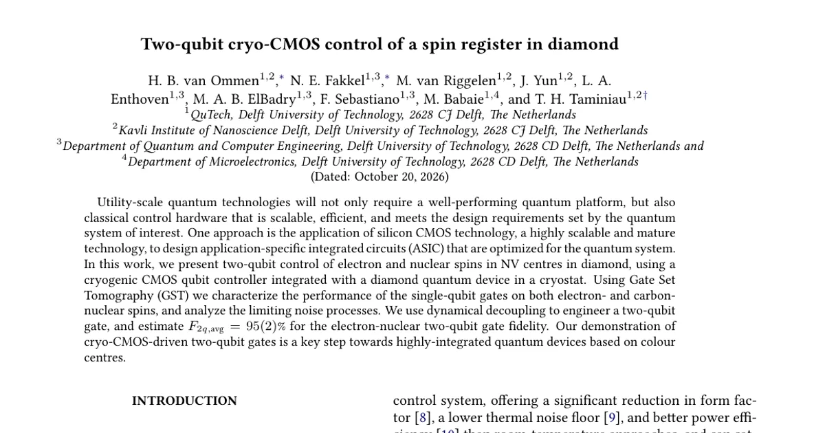
Utility-scale quantum technologies will not only require a well-performing quantum platform, but also classical control hardware that is scalable, efficient, and meets the design requirements set by the quantum system of interest. One approach is the application of silicon CMOS technology, a highly scalable and mature technology, to design application-specific integrated circuits (ASIC) that are optimized for the quantum system. In this work, we present two-qubit control of electron and nuclear spins in NV centres in diamond, using a cryogenic CMOS qubit controller integrated with a diamond quantum device in a cryostat. Using Gate Set Tomography (GST) we characterize the performance of the single-qubit gates on both electron- and carbon nuclear spins, and analyze the limiting noise processes. We use dynamical decoupling to engineer a two-qubit gate, and estimate $F_\text{2q,avg} = 95(2)\%$ for the electron-nuclear two-qubit gate fidelity. Our demonstration of cryo-CMOS-driven two-qubit gates is a key step towards highly-integrated quantum devices based on colour centres.