Research
Scaling Alternating-Bias-Assisted Annealing for Precision Transmon Frequency Targeting on Superconducting Quantum Processors
Overview Research area: Superconducting quantum computing hardware — specifically, post-fabrication Josephson-junction trimming for precision qubit frequency targeting on transmon-based quantum proces
- arXiv
- 2608.27789
- Published
- 2026-08-27
- Authors
- Xiqiao Wang, Mark Field, Teng Zhang, Xian Wu, Ferhat Aydinoglu, Joel Howard, Angela Q. Chen, Sara Elzeiny, Robert Smith, Timothy McSorley, Nicholas Sharac, Eyob Sete, Alysson Gold, Hilal Cansizoglu, Greg Stiehl, Josh Mutus, Kameshwar Yadavalli, Andrew Bestwick, Stefano Poletto, Raja Katta, David P. Pappas
AI summary
Overview
Research area: Superconducting quantum computing hardware — specifically, post-fabrication Josephson-junction trimming for precision qubit frequency targeting on transmon-based quantum processors.
Technical level: Advanced (assumes familiarity with transmons, Josephson junctions, CZ gates, and randomized benchmarking, though the core argument is followable by an intermediate reader).
Scope: A wafer-scale and processor-scale experimental study of alternating-bias-assisted annealing (ABAA) as a production technique for narrowing qubit frequency distributions, covering throughput scaling, yield, process control, aging, and a demonstration on a 36-qubit modular processor.
What This Paper Is About
Building a superconducting quantum processor requires every qubit to sit at a frequency chosen by the Hamiltonian design, but as-fabricated Josephson junction resistances vary by roughly 3% in resistance, which translates to large frequency errors. The authors take a post-fabrication trimming method — ABAA — and show it can be run at wafer scale in parallel across many channels, characterize what limits its yield and speed, and demonstrate it on a real multi-chip processor. The goal is to establish ABAA as a foundry-compatible, scalable enabler for high-precision Hamiltonian targeting in modular quantum processors.
Key Contributions
-
Wafer-scale, multi-channel ABAA demonstration. The authors implement simultaneous parallel ABAA using multi-channel source measure units and cantilever probe cards, tuning 9, 18, and 27 components per probe-card touchdown, and demonstrate a wafer-scale junction resistance tuning precision of σ = 0.50 ± 0.05% with a component-level yield ≥ 98.8%.
-
Throughput scaling analysis with projections. Throughput gain is measured experimentally at 9, 18, and 27 channels (median gain ~4.5 at 9 channels) and extrapolated to 108 channels — equivalent to a full 36Q QPU in a single touchdown — projecting approximately 30-fold throughput gain despite sub-linear scaling.
-
Identification of junction breakdown voltage (BDV) as a process control parameter. The paper quantifies the exponential dependence of both short probability per annealing pulse and tuning time on wafer-median BDV across a range of annealing voltages, and implements a feedforward/feedback control strategy using BDV measured on test devices to select annealing voltage.
-
Processor-level frequency targeting demonstration. ABAA is implemented on the Rigetti Cepheus-1-36Q™ quad-module processor, achieving an empirical targeting precision of ~30 MHz (1σ) in both qubit frequency and qubit-qubit detuning, and a correlation is observed between tighter detuning targeting and higher maximum two-qubit gate fidelities.
Main Findings
-
Wafer-scale precision and yield: Across the parallel-ABAA wafers (14 wafers), post-ABAA resistance spread was σ = 0.50 ± 0.05% with mean offset 0.13 ± 0.38%, compared with a pre-ABAA spread of 3.3 ± 0.4%. Serial ABAA (10 wafers) gave σ = 0.53 ± 0.06%, indicating parallel operation does not degrade targeting precision.
-
Component-level yield: In the detailed 150-mm wafer example, 136 nine-qubit (9Q) chiplets were fabricated; 83 passed screening and 747 qubits were tuned using approximately 1.6 million alternating annealing voltage steps. Nine qubits shorted, giving 89% chiplet-level yield and 98.8% component-level yield, with a short probability per annealing pulse of ~6 × 10⁻⁶.
-
Temporal aging over 14 weeks: Stored at room temperature in a nitrogen-purged environment, the wafer-level resistance offset drifted to approximately 2%, and the 1-σ spread widened from 0.4% to approximately 0.9%. Chip-level median spread grew from 0.25% (~6 MHz predicted) to ~13 MHz, and wafer-level spread from 0.5% (~11 MHz) to ~23 MHz — a degradation factor of roughly 2.
-
Sub-linear throughput scaling: At 9 parallel channels the median throughput gain is ~4.5, roughly half the channel count, and gain deviates further below the y = 0.5x guideline as channel count rises because the slowest component dictates total touchdown duration.
-
Extreme sensitivity to breakdown voltage: Along the 0.86 V operational line, a ~100 mV (~9%) decrease in BDV (from 1160 mV to 1060 mV) increases the short probability by more than two orders of magnitude. Tuning time at a 15% active tuning distance increases exponentially with BDV at fixed annealing voltage, and also increases exponentially when annealing voltage is reduced (shown for a wafer with median BDV ~1.12 V).
-
Defect-free lattice projection: Assuming a maximum capacity of 212 9Q chiplets per 150-mm wafer and the 89% chiplet-level yield from the example, the authors project 188 short-free 9Q chiplets, interconnectable into a defect-free lattice of >1600 qubits.
-
Processor-level resistance targeting: On Cepheus-1-36Q™, resistance deviation improved from μ ± σ = −11.32 ± 3.55% before ABAA to 0.39 ± 0.49% after ABAA.
-
Processor-level frequency targeting: Predicted f₀₁ᵐᵃˣ error improved from 294 ± 106 MHz to 9 ± 12 MHz (a ~9-fold reduction in spread), while the measured error after cooldown at ~10 mK was 132 ± 30 MHz. Predicted qubit-qubit detuning error improved from 51 ± 123 MHz to 2 ± 11 MHz; the measured detuning error was 1 ± 32 MHz, with negligible global offset.
-
Detuning accuracy is preserved: Because global offsets in absolute f₀₁ᵐᵃˣ cancel when computing detunings, the detuning offset remains small even though the absolute frequency offset is large; no significant difference was observed between TC and IMC edges.
-
Gate fidelity correlation: Adiabatic-CZ fidelity, benchmarked via interleaved randomized benchmarking across all 48 TC edges and the live IMC edges (reported as 11 in the figure caption and 12 in the text), shows higher maximum fidelities for edges whose detunings are tuned closer to the design target. The processor achieved a median two-qubit (CZ) gate fidelity of 99.5% and was first deployed for public access in August 2025.
Methodology in Plain English
Each annealing cycle has four steps: apply a positive annealing voltage, monitor resistance at a small bias, apply a negative annealing voltage of the same magnitude, monitor again. Monitoring at low bias, in the linear I–V regime, gives real-time feedback on the junction resistance. During active tuning, resistance rises logarithmically with cycle count; after the last pulse, it continues to creep upward following a power law. The protocol therefore does not stop at the target — it stops at a calibrated threshold below the target and lets the junction relax into place during a defined aging window.
Before tuning, chiplets are screened out if their junctions are too close to the target from below (under 3%, leaving insufficient room for relaxation), above the target (tuning is upward-only), or more than roughly 25% below the target (which would require impractically long tuning given the logarithmic slowdown). On the example wafer, an intentional global offset of about −12% was built in to leave headroom.
To scale throughput, the team used multi-channel source measure units and a cantilever probe-card array to anneal many components at once, so that a single touchdown tunes, for example, 27 qubits, couplers, and inter-module couplers simultaneously. Throughput gain is computed as the summed tuning time of all components divided by the time of the slowest one.
For process control, the authors measured breakdown voltage on a dedicated set of test qubit devices on each wafer before tuning, then used phase diagrams of short probability and tuning time versus BDV and annealing voltage to pick an operating point.
Finally, frequency is predicted from room-temperature resistance using an empirical Ambegaokar–Baratoff relation (E_J,est = α_AB / R_N) combined with simulated charging and Josephson energies, so that post-ABAA resistance distributions can be converted into predicted frequency distributions and compared against cryogenic measurements and gate benchmarks.
Why This Matters
Impact on research. The paper moves ABAA from a laboratory demonstration to a characterized production process, and shows that the key fabrication lever for tuning yield and speed is junction breakdown voltage — a measurable, controllable quantity tied to barrier oxidation. It also separates the error budget into distinct parts (resistance targeting, aging, frequency prediction, thermal cycling), which gives the field a quantitative map of where the remaining targeting error comes from. The demonstration that detuning accuracy survives even when absolute frequency has a global offset is practically important for modular architectures.
Real-world applications (as implied by the paper's framing):
- Fabrication of large-scale superconducting quantum processors with designed frequency allocations.
- Modular processor assembly, where multiple 9Q chiplets are tiled into larger defect-free lattices.
- Semiconductor-style test and measurement workflows (probe cards, multi-channel SMUs) applied to quantum device production.
- Calibration automation for processors hosting large numbers of qubits, where tight frequency targeting simplifies gate and measurement calibration.
Industry relevance. The technique requires only commercially available electrical test equipment, runs at room temperature, and is compatible with existing foundry and packaging infrastructure — all of which the authors emphasize as advantages over laser annealing. The BDV-based control loop addresses manufacturing variability directly, which is the kind of process-control argument that matters for yield planning.
Future Directions
-
Improving frequency prediction models. The measured f₀₁ᵐᵃˣ error (132 ± 30 MHz) is far larger than the post-ABAA prediction (9 ± 12 MHz); the authors attribute this to finite accuracy in simulated shunt capacitance, wafer-to-wafer variation in the empirical Ambegaokar–Baratoff coefficient, and resistance changes during post-ABAA processing and thermal cycling, and state that they are refining electromagnetic simulations and working to control that coefficient.
-
Understanding and controlling pre-cooldown resistance drift. The paper identifies aging between tuning and measurement as a major error source and suggests on-demand ABAA or cryogenic storage as mitigations.
-
Mitigating wafer-to-wafer global offsets when interconnecting chiplets from multiple wafers into large-scale modular processors.
-
Pushing yield higher while preserving throughput. The 98.8% component-level yield is described as insufficient for a defect-free monolithic QPU beyond the 100-qubit scale, so further suppression of short probability (e.g., lower annealing voltage, offset by more parallel channels) remains an open engineering question.
Target Audience
Process and hardware engineers working on superconducting qubit fabrication and test; quantum computing researchers interested in Hamiltonian targeting, frequency crowding, and two-qubit gate optimization; and technical readers evaluating the manufacturability and scalability of modular superconducting processor architectures. Readers without background in Josephson junctions or transmon physics will find the device-level details dense, but the yield, throughput, and process-control framing is accessible to anyone in semiconductor manufacturing or quantum engineering.
Authors’ abstract
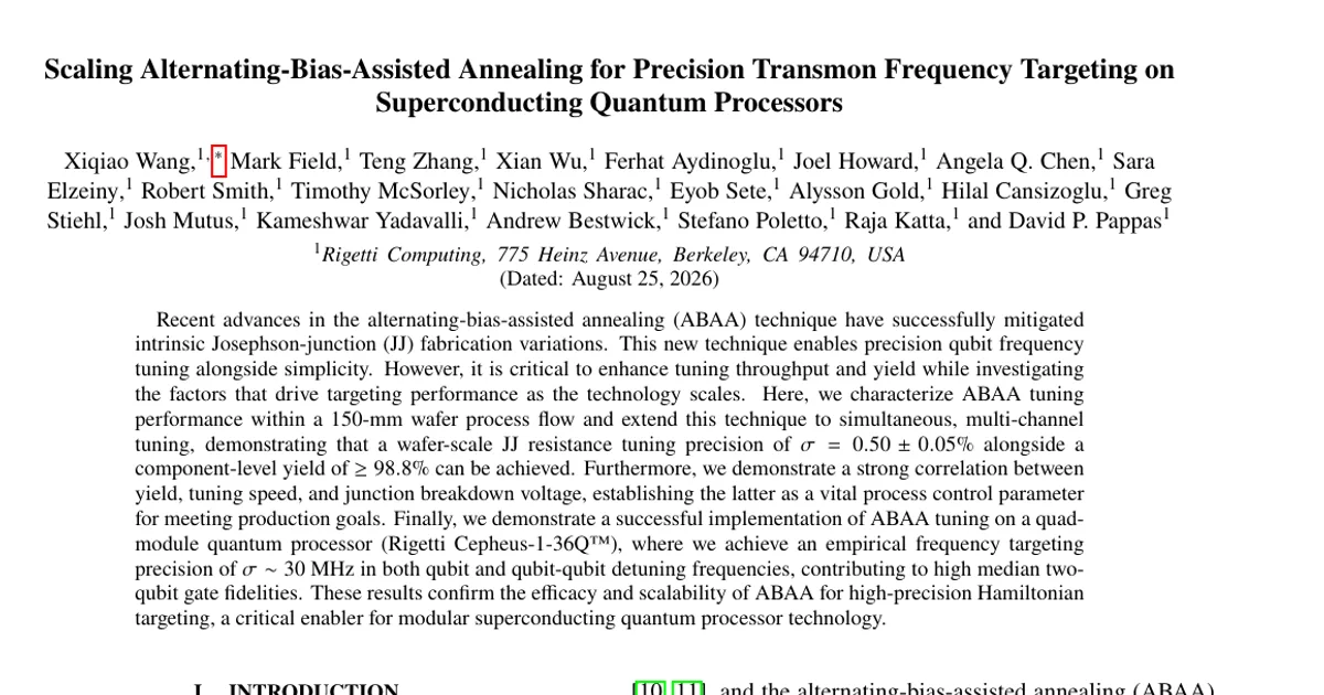
Recent advances in the alternating-bias-assisted annealing (ABAA) technique have successfully mitigated intrinsic Josephson-junction (JJ) fabrication variations. This new technique enables precision qubit frequency tuning alongside simplicity. However, it is critical to enhance tuning throughput and yield while investigating the factors that drive targeting performance as the technology scales. Here, we characterize ABAA tuning performance within a 150-mm wafer process flow and extend this technique to simultaneous, multi-channel tuning, demonstrating that a wafer-scale JJ resistance tuning precision of $σ=0.50\pm0.05\%$ alongside a component-level yield of $\ge 98.8\%$ can be achieved. Furthermore, we demonstrate a strong correlation between yield, tuning speed, and junction breakdown voltage, establishing the latter as a vital process control parameter for meeting production goals. Finally, we demonstrate a successful implementation of ABAA tuning on a quad-module quantum processor (Rigetti Cepheus-1-36Q), where we achieve an empirical frequency targeting precision of $σ\sim 30\text{ MHz}$ in both qubit and qubit-qubit detuning frequencies, contributing to high median two-qubit gate fidelities. These results confirm the efficacy and scalability of ABAA for high-precision Hamiltonian targeting, a critical enabler for modular superconducting quantum processor technology.