The Signal
Wolfspeed Offers Transparent SiC for Quantum-Computing Applications
Wolfspeed says its optical-grade transparent silicon carbide substrates are commercially available for optical applications, with quantum computing among the areas being explored. Its announcement describes a material platform, not demonstr
Quantum.world Team · Written with AI · fact-checked ·
Wolfspeed is selling transparent silicon carbide wafers for optical applications, including quantum computing, but its announcement offers a material platform—not a demonstrated quantum device. The distinction matters: the company presents SiC as a crystal that can host qubits and carry quantum information in light, while reporting no quantum-device performance results alongside the commercial launch.
From quantum potential to a product listing
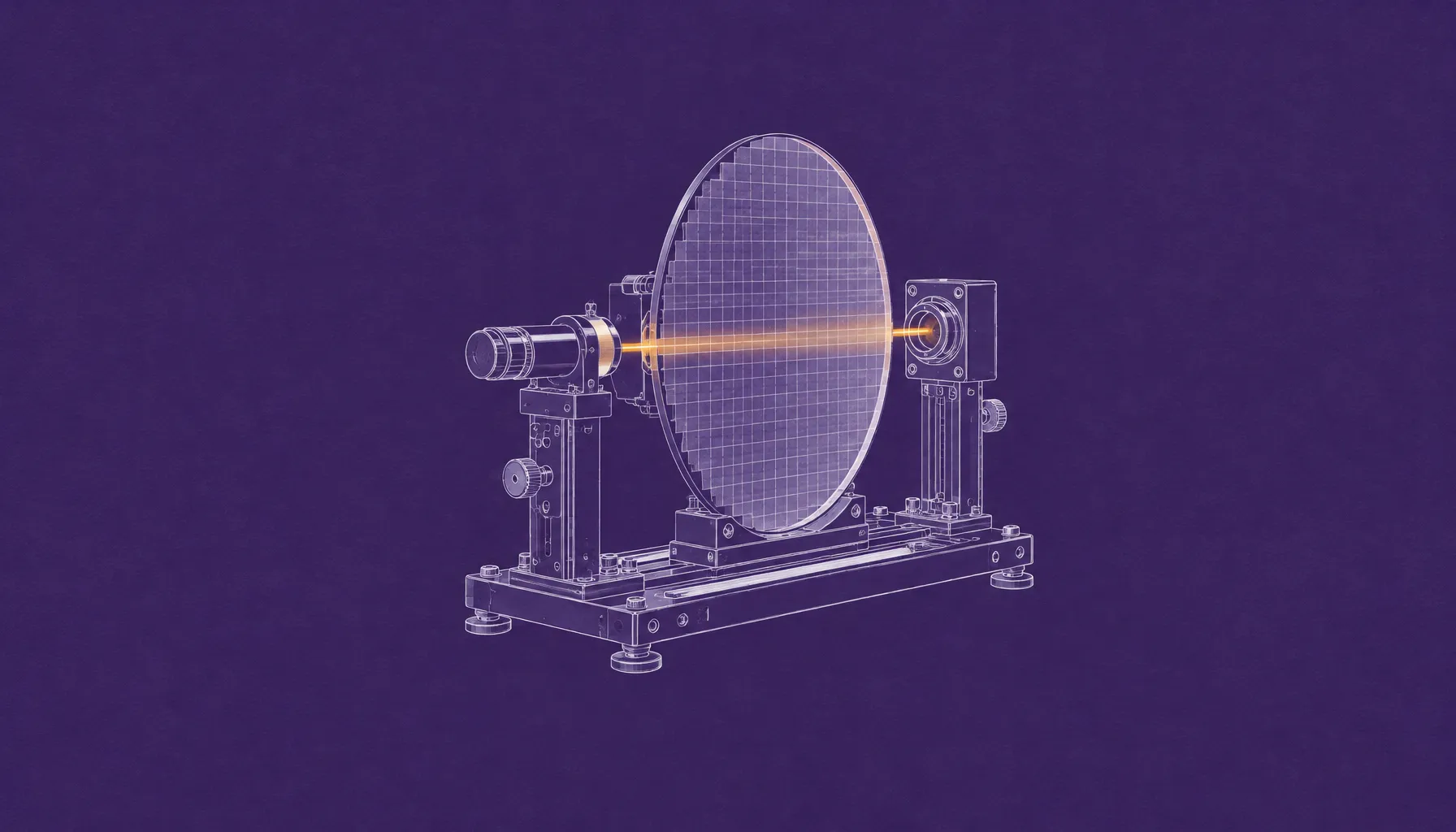
Wolfspeed announced the commercial introduction of its transparent silicon carbide technology, branded TSiC™, on October 29. The company says the optical-grade substrates are engineered for low optical absorption and wafer flatness, and identifies augmented-reality waveguides and quantum computing as potential applications.
“Our proprietary TSiC™ technology and extensive intellectual property portfolio position us to help enable breakthroughs in augmented reality, quantum computing and other emerging markets, reinforcing the versatility and transformative potential of silicon carbide.”
Katrin Feurle, Vice President, Beyond Power at Wolfspeed
The company describes a possible quantum use in which one SiC crystal hosts qubits, preserves their quantum states and transmits quantum information through light. That is Wolfspeed’s account of the material’s potential; the announcement does not report a processor, a fabricated quantum device, or qubit measurements.
150 mm and 200 mm wafers are listed
Wolfspeed’s product page lists 150 mm and 200 mm substrates as commercially available. It identifies them as double-side-polished, on-axis 4H-SiC wafers and gives separate product numbers for the two diameters.
The listed target specifications include a thickness of 500 micrometres, with a tolerance of 20 micrometres, and an absorption coefficient no greater than 0.05 cm-1 across wavelengths from 450 to 650 nanometres. The page also specifies total thickness variation of no more than 1.5 micrometres, with a 3 mm edge exclusion, and optical roughness of no more than 1 nanometre on both sides. Wolfspeed cautions that specifications may vary by diameter.
The 300 mm format is not presented on the same footing as the commercial 150 mm and 200 mm offerings. The product page describes 300 mm as in sampling or available on request; the announcement says the company continues developing 300 mm TSiC technology.
A substrate does not settle the device question
For quantum developers, the announcement makes the wafer supply more concrete, but it leaves device-level questions unanswered. Wolfspeed provides no quantum yield, coherence, gate-fidelity, or shipment data in the release. Nor does it name a quantum-computing customer or disclose wafer pricing.
Silicon carbide’s optical properties and its ability to host spin defects are part of the company’s case for the material. The commercial introduction establishes that Wolfspeed is offering optical-grade substrates for that work; it does not establish that the fabrication and integration steps needed for a quantum system have been completed.
300 mm remains the next size under development
Wolfspeed says its work builds on more than 35 years of silicon carbide development and experience producing high-purity semi-insulating wafers. For now, the clearest commercial distinction is by diameter: 150 mm and 200 mm substrates are listed as available, while 300 mm remains at the sampling or request stage.